Additive diffractive optical elements fabrication by PECVP deposition of SiO2 and lift-off process

Abstract
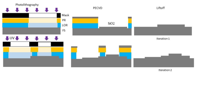
Diffractive optical elements (DOEs) gradually start replacing traditional refractive optics in many applications. The growing interest in DOEs is mainly because of their flexibility in light manipulation with a small form factor and their ability to combine simultaneously optical and computational functions into a single part by applying the software-hardware co-design approach. Two main methods are widely used to fabricate DOEs. The first method is the etched-based method that combines photolithography and reactive-ion etching (RIE). The second method is additive fabrication, which combines metal deposition and nanoimprinting (NIL). Both methods have many drawbacks. The RIE methods suffer from issues like lags in the etched depth when the feature sizes differ in the same pattern (RIE lags), high surface roughness, and aspect ratio-dependent etching rate. The second method could produce high-resolution micro-optics. However, the technique could suffer from poor adhesion of the patterns with the substrate and poor uniformity across large areas. Here we propose a new way to fabricate multi-level DOEs by directly growing an optically transparent material on a glass substrate. The method combines the deposition of Silicon dioxide (SiO2) by Plasma-enhanced chemical vapor deposition technique (PECVD) and bi-layer lift-off. We provide evidence of the effectiveness of the fabrication method by comparing a 16-level Fresnel lens fabricated by the RIE method with another lens fabricated by the proposed method. The characterization results show that with the proposed method, the surface roughness is lower, and the depth is uniform. Furthermore, the optical test shows a reduced haze effect.